Electronics engineers and materials scientists have been trying to identify materials that could help to boost the performance of electronics further, overcoming the inherent limitations of silicon-based transistors. Two-dimensional (2D) semiconductors have advantageous properties that make them promising candidates for the development of better performing transistors.
Most notably, 2D semiconductors are atomically thick and exhibit high carrier mobilities, two qualities that could improve the electrostatic control and ON-state performances of short-channel field-effect transistors (FETs). Despite their advantages, these materials exhibit high contact resistances linked to so-called Fermi-level-pinning effects, which significantly reduce their performance in transistors.
Researchers at Peking University and Chinese Academy of Sciences recently introduced a new yttrium-doping strategy that could help to overcome this key limitation of 2D semiconductors, facilitating their effective integration in electronics.
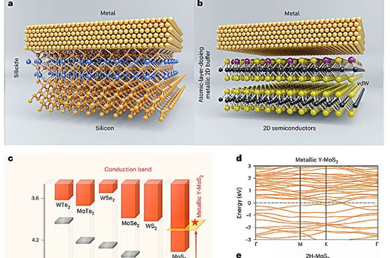
This strategy, outlined in a paper published in Nature Electronics, can convert semiconducting molybdenum disulfide (MoS2) into metallic MoS2, improving band alignment and facilitating the use of MoS2 for fabricating ohmic contacts for 2D transistors.
“We placed a semi-metal layer between a metal electrode and a two-dimensional semiconductor,” Chenguang Qiu, co-author of the paper, told Tech Xplore. “This semi-metal layer enhances the efficiency of carrier injection from the metal electrode to the two-dimensional semiconductor. This idea is inspired by the traditional silicide structure in silicon-based transistors.”
The key goal of the recent study by Qiu and his colleagues was to address the issue of Fermi-level pinning effects at the interface between metal and 2D semiconductor layers in 2D transistors. This is a critical bottleneck in the development of 2D electronics, which has so far prevented their future large-scale fabrication.
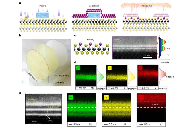
“We have developed the plasma-deposition-annealing (PDA) method to achieve yttrium doping in the surface layer of MoS2,” Qiu said. “First, the patterned local contact areas were treated with low-power soft plasma to generate active sites. Next, a Y/Ti/Au stacked metal was deposited, and the 1 nm-thick active metal Y was used as a solid-state doping source.”

The Y atoms used to dope MoS2 diffuse into the active sites generated using low-power plasma. The researchers then activated them in the top layer of the material, using high-temperature annealing in an inert gas environment.
“Due to the preparation of hyperfine patterned structures, great thermal stability after annealing, and the all-solid-state nature, this PDA doping process is compatible with advanced-node wafer-scale integration,” Qiu said.
In their paper, the researchers introduced a new concept, which they refer to as “rare earth element yttrium doping-induced 2D phase transition.” This phase transition is essentially the metallization that they observed when they applied their yttrium doping strategy to MoS2.
“We have invented a selective-area single-atomic-layer surface doping technique,” Qiu said. “This breakthrough overcomes the traditional engineering limitation where the junction depth of ion implantation doping cannot be less than 5 nanometers, achieving for the first time a doping depth pushed to the atomic layer limit of 0.5 nanometers.”
Using their yttrium-doping strategy, Qiu and his colleagues developed ultra-short MoS2-based channel ballistic transistors that performed well as ohmic contacts and had great switching capabilities. In the future, these transistors could contribute to the development of new sub-1 nanometer node chips that can attain remarkable performances while consuming less power than conventional chips.
“We now hope to develop equally excellent p-type ohmic contacts suitable for 2D semiconductors,” Qiu added. “This would enable the fabrication of complementary symmetrical CMOS transistors, which can be used to build higher performance and lower power consumption large-scale integrated circuits.”
More information:
Jianfeng Jiang et al, Yttrium-doping-induced metallization of molybdenum disulfide for ohmic contacts in two-dimensional transistors, Nature Electronics (2024). DOI: 10.1038/s41928-024-01176-2
© 2024 Science X Network
Citation:
New yttrium-doping strategy enhances 2D transistors (2024, June 25)
retrieved 25 June 2024
from https://techxplore.com/news/2024-06-yttrium-doping-strategy-2d-transistors.html
This document is subject to copyright. Apart from any fair dealing for the purpose of private study or research, no
part may be reproduced without the written permission. The content is provided for information purposes only.


